P-N Junctions
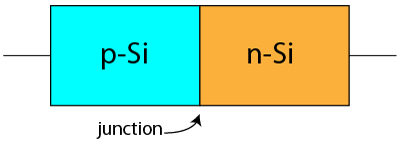
When p-type silicon is placed in close contact with n-type silicon (in what is known as a metallurgical junction), a p-n junction is formed. P-N junctions are electrical devices more commonly known as diodes. Through careful analysis of the junction, you can build a qualitative understanding of how these devices operate.
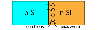
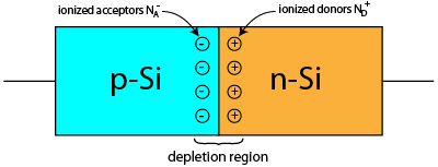
Free electrons on the n-side of the junction diffuse across the junction into the p-side, leaving behind positively ionized donor atoms (ND+) as they slide into the vacancies that were previously holes. This means the electrons have disappeared in the p-type silicon and leaves the n-type silicon region close to the junction with a net positive charge.
In similar fashion, holes on the p-side of the junction diffuse across the junction into the n-side, leaving behind negatively ionized acceptor atoms (NA-) The region close to the junction in the p-type silicon picks up a net negative charge. The holes disappear in the n-type silicon because of all the free electrons.
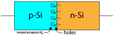
Because the free charges near the junction have crossed the junction and been absorbed by the dopant atoms, there is a deficiency of free charges near the junction. This region is known as the depletion region, because it is depleted of free carriers. You may also hear it referred to as the space charge region, because it is a region of positive donor charges and negative acceptor charges separated by space.
The depletion region on the p-side of the junction is negatively charged because the dopant acceptor atoms picked up electrons, and the depletion region on the n-side of the junction is positively charged because the dopant donor atoms lost their electrons. Note that the ionized dopant atoms are not free to move, unlike the electrons and holes, because the dopants are held in place in the crystal lattice.
The fixed charges in the depletion region set up a small electric field pointing from the positive side to the negative side. This is known as the built-in electric field (εbi).
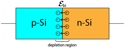
In the bulk of the p-n junction, away from the depletion region, the abundance of free carriers capable of transporting charge makes the regions good conductors. In the small depletion region near the junction, however, the absence of free carriers makes the depletion region a good insulator. Further, positive charge carriers (holes) from the p-side bulk that wander near the depletion region get pushed back into the p-side bulk by the built-in electric field. Likewise, negative charge carriers (electrons) from the n-side bulk wandering near the depletion region are pushed back into the n-side bulk. The net effect is that current cannot flow from the p-side to the n-side of the diode. Carriers that try to diffuse will be returned by the electric field.
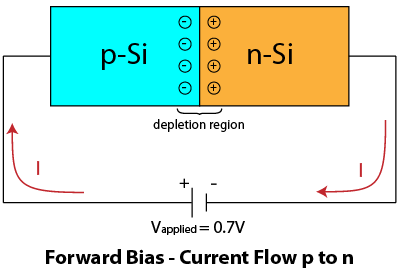
When a potential difference of approximately 0.7 volts or greater is applied to the circuit, however, with the positive side of the applied voltage connected to the p-side of the diode, the applied voltage counteracts the built-in field in the depletion region, and charge carriers can again flow across the junction by diffusion, allowing positive current flow from the p-side to the n-side of the diode. This is known as applying a forward bias to the diode.
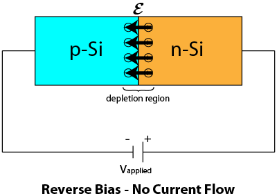
If a potential difference (voltage) is applied in the opposite direction, however, with the positive side of the applied voltage attached to the n-side of the diode, the applied voltage enhances the built-in field in the diode, preventing current flow and making the diode an even better insulator. This is known as applying a reverse bias to the diode.
Question: An n-type semiconductor and a p-type semiconductor are joined to form a diode. Compared to the total number of electrons in the semiconductors before joining, the number of electrons in the diode is
- fewer
- greater
- the same
Answer: (3) the same due to the law of conservation of charge.
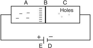
Question: Using the diagram, answer the following questions
A. In the diagram, C represents
- n-type silicon
- p-type silicon
- anode
- diode
B. The p-n junction in the diagram is biased
- reverse
- forward
- A to E
- C to D
Answers:
A. (2) p-type silicon (you can tell because of all the holes!)
B. (1) the p-n junction is reverse biased.
Question: Compared to the current flow when a forward bias is applied to a p-n junction, the current flow when a reverse bias is applied to a p-n junction is
- less
- greater
- the same
Answer: (1) the current through a reverse-biased p-n junction is minimal.
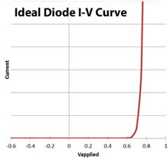
Putting this all together, you can make a graph of the current through a diode as a function of the applied potential difference Vapp. This is known as an I-V curve, where I is current and V is the applied potential difference.
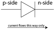
As you can see from the diode's I-V curve, the diode acts like a one-way gate for current, allowing current to flow through in one direction only (from p to n). For this reason, the circuit symbol for a diode indicates the direction current can flow from p to n with an arrow, and shows a line blocking current from n to p.
When placed in a circuit, a diode acts as an insulator, or open, until the diode is given a forward bias of approximately 0.7 volts, at which point it acts in a fashion similar to a very low resistance wire. Circuit analysis of a diode, therefore, can be quite straightforward.
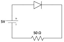
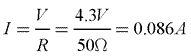
Question: Find the current flowing in the circuit at right. Assume the diode turns on at exactly 0.7 volts of forward bias.
Answer: Because the voltage source provides more than 5V of forward bias, you can assume the diode is turned on. Therefore, the voltage drop across the diode must be 0.7 volts, leaving 4.3 volts to drop across the resistor. You can find the current through the resistor (and therefore through the entire circuit since the circuit is in series) using Ohm's Law.