
Transistors
What happens when two diodes are placed back-to-back in a p-n-p configuration, as shown in the diagram below?
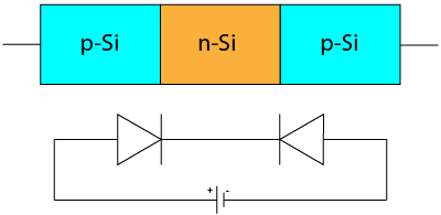
Current cannot flow. Because a diode acts like a one-way gate for current, whichever direction current comes from, one of the diodes is reverse biased, cutting off current flow through the circuit. But, what if you could selectively modify the center region?
By placing a second, negative potential near the n-type silicon region, electrons near the negative potential will be repelled, creating another depletion region in the n-type silicon.
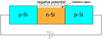
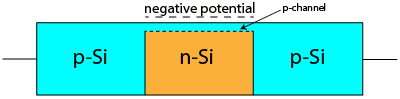
As the depletion region grows, the bias across the p-n junction on the left approaches 0.7 V and the holes in the p-type silicon enter the depleted n-region. The holes stay near the surface and form a channel across the n-Si to the p-Si on the right. This is known as a p-channel inside the n-type silicon, as you have "inverted" the silicon.
You now have a complete p-type silicon path with ample charge carriers, therefore current can flow through the device. The p-n-p device is now acting like a controllable gateway for current, and the negative potential is the switch (or gate) to turn on and off the current flow from what is known as the source side of the device to the drain side of the device, as shown below.
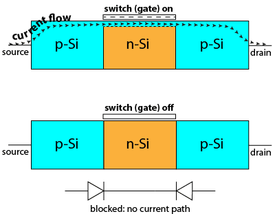
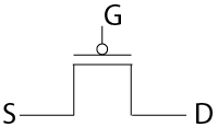
This p-n-p device, with three contacts (source of current, drain of current, and gate switch), is known as a field effect transistor, or FET. The circuit schematic symbol for a pnp FET indicates the source, gate, and drain of the device, as shown below.
Note that there are a number of other types and modifications of FETs, including devices made out of n-p-n junctions. For purposes of simplicity, this book will focus solely on the p-n-p device described. Readers are referred to more detailed texts on microelectronic technology and digital logic for a more thorough and complete background.